PCB Creepage vs. Clearance: Differences, Requirements and Design Guidelines
A PCB can pass connectivity tests yet fail insulation safety requirements. This article explains the difference between creepage and clearance distances, why they matter, and how voltage, environmental conditions and PCB geometry influence safe insulation design in power supplies and industrial electronics.

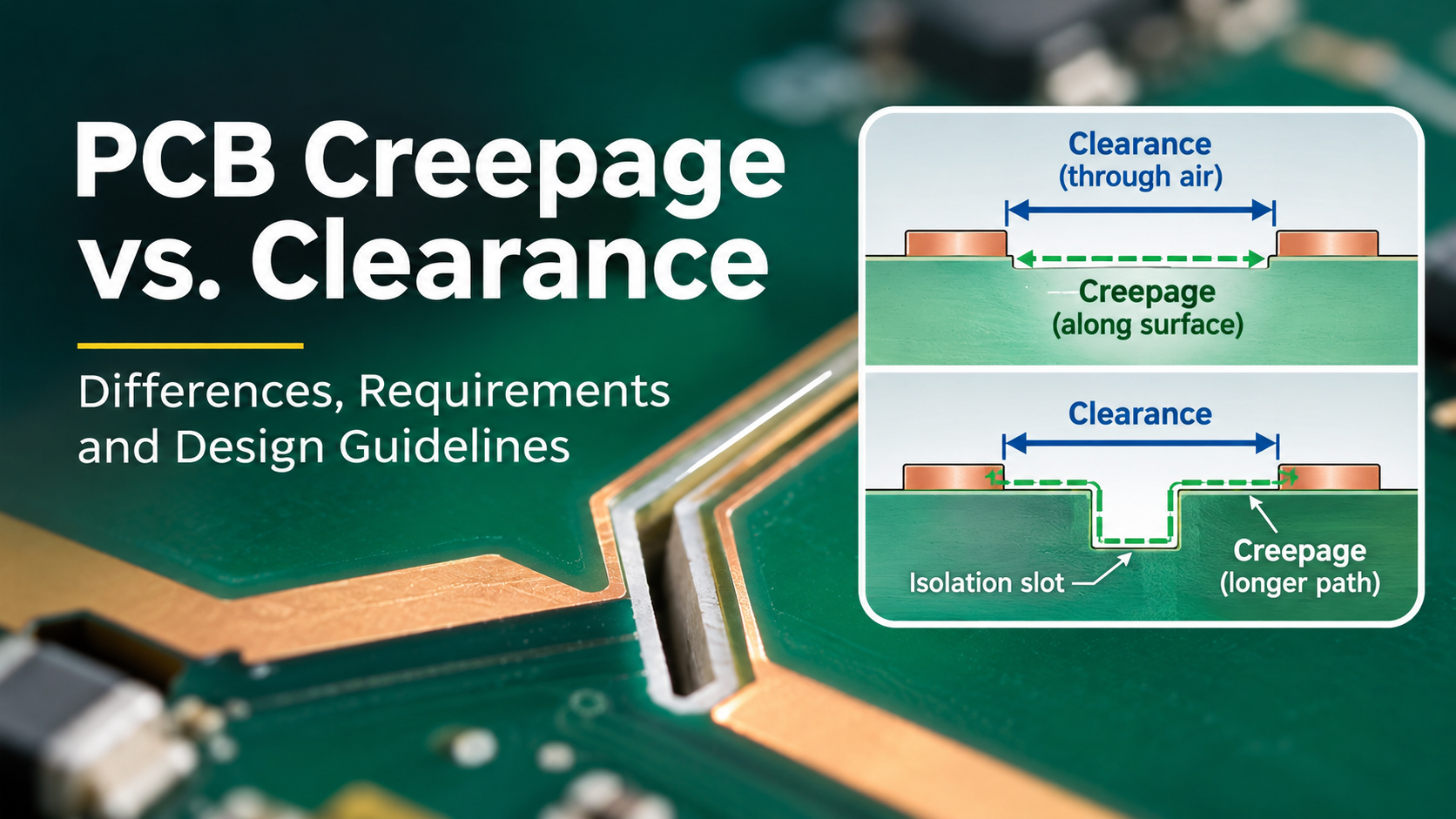
1. What Is the Difference Between Creepage and Clearance?
Both measurements describe the separation between conductive parts at different electrical potentials. However, the path used to measure each distance is different.
Clearance distance is the shortest distance through air between two conductive parts. It determines how much air insulation is available to withstand an electrical potential difference without flashover or breakdown.
Creepage distance is the shortest distance along the surface of an insulating material between two conductive parts. It addresses the possibility of leakage current, surface discharge and eventual insulation failure along the PCB substrate.
The distinction becomes important because air and solid insulating materials behave differently under electrical stress. A spacing arrangement that provides adequate separation through air does not necessarily provide sufficient protection against surface-related insulation failure.
Understanding the two paths
Consider two copper traces placed on the same PCB layer. The clearance measurement follows the shortest available route through the air between their exposed conductive edges. The creepage measurement follows the insulating surface separating those traces.
On a flat, unobstructed PCB surface, the two distances may be numerically similar. However, the situation changes when the board contains slots, barriers, grooves, component bodies or other physical features.
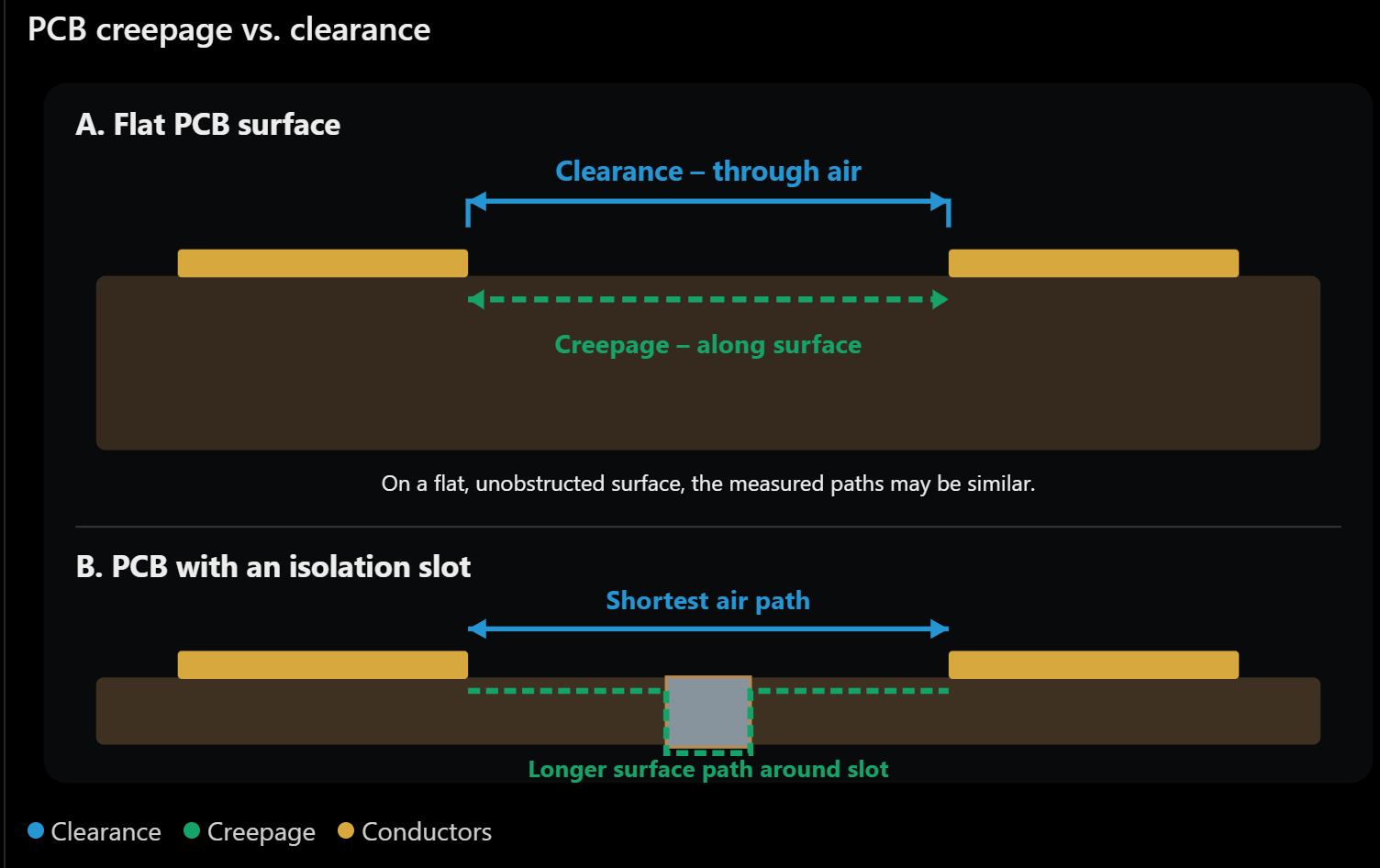
A useful way to remember the distinction is:
- Clearance concerns the electrical separation through air.
- Creepage concerns the electrical separation along an insulating surface.
Neither measurement can automatically replace the other. A design must satisfy both applicable requirements.
2. Why Creepage and Clearance Have Different Safety Requirements
The two distances address different failure mechanisms, which is why insulation coordination standards treat them separately.
Clearance: preventing electrical breakdown through air
Air provides insulation under normal operating conditions, but its dielectric strength is not constant under every environmental and electrical condition.
A sufficiently high electric field can ionize the air between conductors, allowing an electrical discharge to develop. This can result in flashover between PCB tracks, terminals or other conductive components.
The required clearance therefore depends on several factors, including:
- Rated impulse withstand voltage: The transient voltage that the insulation system must withstand under the applicable test conditions.
- Overvoltage category: The expected transient overvoltage environment associated with the equipment's connection to the electrical supply.
- Altitude: Atmospheric pressure decreases with increasing altitude, which can reduce the dielectric strength of air and increase the required clearance.
- Insulation type: Basic, supplementary and reinforced insulation have different safety objectives and requirements.
- Electric field geometry: The shape and arrangement of conductors influence the local electric field and potential discharge points.
This explains why clearance should not be calculated using only the nominal DC voltage printed on a circuit diagram.
A power converter operating from a nominal DC bus, for example, may experience transient conditions that are significantly different from its steady-state voltage. The insulation design must account for the relevant electrical stresses specified by the applicable product safety standard.
Creepage: preventing surface-related insulation failure
Creepage focuses on the insulating surface separating two conductive regions.
Unlike a clearance failure, which involves an electrical discharge through air, creepage-related problems can develop through contamination, moisture and degradation of the insulating surface.
When conductive contamination accumulates on a PCB, it can create a path for leakage current. Under sustained electrical stress, this can contribute to surface deterioration and the formation of conductive tracks.
This process is commonly associated with electrical tracking.
Several environmental and material properties influence creepage requirements:
- Pollution degree: Describes the expected contamination conditions in the equipment's microenvironment.
- Material group: The electrical tracking characteristics of the insulating material influence the creepage requirements.
- Working voltage: The relevant voltage stress across the insulation influences the required creepage distance.
- Insulation type: The required level of protection affects the applicable distance.
- Humidity and condensation: Moisture can increase surface conductivity and aggravate leakage-related problems.
The important point is that creepage is not simply another way of measuring physical separation. It accounts for the condition and electrical properties of the insulating surface itself.
3. The Role of CTI and PCB Material Selection
PCB substrate selection is an important part of insulation design.
One material property used in creepage-related evaluations is the Comparative Tracking Index (CTI). It is determined through a standardized test that evaluates the resistance of an insulating material to electrical tracking under specified test conditions.
Materials are assigned CTI values and corresponding material groups under the applicable insulation coordination framework.
A higher CTI generally indicates better resistance to tracking in this test.
For example, two PCB substrates with similar mechanical and thermal characteristics may have different CTI classifications. Their creepage requirements can consequently differ under the same insulation coordination conditions.
This is one reason why simply specifying FR-4 does not provide enough information to complete a safety spacing assessment. The actual laminate specification and its recognized material properties matter.
Material group classifications are commonly associated with the following CTI ranges:
| Material group | CTI value |
|---|---|
| Group I | 600 or greater |
| Group II | 400 to below 600 |
| Group IIIa | 175 to below 400 |
| Group IIIb | 100 to below 175 |
These classifications provide a material-based input to creepage evaluation. They do not independently establish a safe PCB spacing.
CTI testing and classification should be considered alongside the other insulation coordination parameters, using the applicable edition of the relevant standard.
4. How Pollution Degree and Humidity Affect Creepage
A PCB designed for a clean, controlled environment may not require the same insulation provisions as one operating in an industrial setting.
Pollution degree is used to describe the contamination conditions expected around the insulation system.
The commonly used classifications are:
- Pollution Degree 1: No pollution or only dry, non-conductive pollution. Any pollution present has no influence on insulation performance.
- Pollution Degree 2: Normally non-conductive pollution, with occasional temporary conductivity caused by condensation.
- Pollution Degree 3: Conductive pollution or dry, non-conductive pollution that becomes conductive because of condensation.
- Pollution Degree 4: Persistent conductivity caused by conductive dust, rain or other wet conditions.
The classification is based on the actual microenvironment around the insulation, not simply whether the equipment is described as industrial or consumer-grade.
For instance, an enclosed electronic controller may operate in a relatively controlled environment. However, an enclosure does not automatically guarantee a lower pollution degree. Dust accumulation, ventilation arrangements, condensation and other conditions still need to be considered.
This is particularly relevant for industrial control boards, outdoor equipment and electronics installed near machinery.
5. Can a PCB Isolation Slot Increase Creepage Distance?
Yes. A correctly designed isolation slot can increase the creepage distance between two conductive regions without requiring the same increase in overall PCB dimensions.
This is one reason slots are commonly considered in high-voltage PCB layouts.
A milled slot removes part of the insulating board material between conductive areas. Instead of following a relatively direct path across the board surface, the creepage path may need to travel down one side of the slot, around its interior and up the opposite side.
The resulting surface path can be longer than the original straight separation.
However, there is an important distinction between increasing creepage and increasing clearance.
The slot can lengthen the surface path, but the shortest air path must still be evaluated independently. The slot does not automatically provide sufficient clearance or eliminate the need to satisfy the applicable insulation requirements.
Its effectiveness depends on several geometric details:
- Slot width and depth.
- The position of the conductive edges relative to the slot.
- PCB thickness and construction.
- The accessible surface path around the slot.
- The measurement rules in the applicable product standard.
A narrow slot should not automatically be treated as a valid creepage extension. Its dimensions and geometry must satisfy the relevant standard's requirements.
In practice, isolation slots can be useful when PCB area is limited, but they should be incorporated during the insulation design stage rather than added as a last-minute layout modification.
6. Does Conformal Coating Reduce Creepage and Clearance Requirements?
Conformal coating is often used to protect electronic assemblies against moisture, dust and environmental contamination.
However, applying a coating does not automatically allow a designer to reduce PCB spacing.
The effectiveness of the coating depends on its insulating properties, application process, coverage, thickness, adhesion, durability and qualification under the applicable standard.
For example, an incomplete coating can leave exposed areas where the original creepage and clearance requirements still apply. Defects, bubbles, contamination and damage during manufacturing or servicing can also compromise the intended protection.
IEC 60664-3 specifically addresses the use of coating, potting and moulding for protection against pollution. It defines requirements and test procedures for qualifying such protective arrangements.
Consequently, a conformal coating should be treated as part of a qualified insulation system, not as a substitute for spacing without supporting evidence.
7. Which Standards Govern PCB Creepage and Clearance?
There is no single spacing table that applies to every PCB design.
The applicable requirements depend on the equipment, insulation function, electrical characteristics and operating environment.
Some important standards include:
IEC 60664-1: Insulation coordination for equipment within low-voltage supply systems
This is a fundamental reference for insulation coordination. It addresses clearances, creepage distances, solid insulation and associated electrical testing.
The standard considers parameters such as rated impulse withstand voltage, pollution degree, material characteristics and altitude.
The 2025 consolidated publication, IEC 60664-1:2020+AMD1:2025, includes updated provisions and tables. Its stated scope covers equipment connected to low-voltage supply systems with rated voltages up to AC 1,000 V or DC 1,500 V, and frequencies up to 30 kHz.
IEC 60664-3: Use of coating, potting or moulding for protection against pollution
This standard addresses qualified protective systems used to protect assemblies against pollution. It is particularly relevant when considering whether a coating or encapsulation system can support modified insulation spacing.
IEC 62368-1: Audio/video, information and communication technology equipment – Part 1: Safety requirements
This is a product safety standard for relevant audio/video and information and communication technology equipment. It defines safety requirements and safeguards based on the energy sources present in the equipment.
It should be used where applicable to the product rather than treated as a universal PCB spacing standard.
The governing product standard should always be identified before selecting spacing values. Product-specific standards may establish additional or different requirements.
8. A Practical Workflow for Reviewing PCB Insulation Spacing
A systematic review is more reliable than checking a few track-to-track distances at the end of the layout process.
The following workflow provides a practical starting point.
Step 1: Identify the insulation boundaries
Mark the areas where insulation is required.
Typical examples include:
- Primary-side to secondary-side isolation.
- Hazardous-voltage circuits to accessible low-voltage circuits.
- Different voltage domains within a power converter.
- Conductors separated by reinforced or supplementary insulation requirements.
Step 2: Identify the governing product standard
Determine which safety standard applies to the complete equipment.
This decision establishes the insulation coordination framework and the applicable measurement rules.
Step 3: Establish the electrical requirements
Identify the relevant working voltage, transient overvoltages, rated impulse withstand voltage and insulation category.
Do not rely solely on the nominal supply voltage.
Step 4: Determine the environmental and material conditions
Establish the pollution degree, altitude, PCB material group and other relevant environmental conditions.
Confirm the actual laminate specification instead of relying on a generic material name.
Step 5: Measure clearance and creepage independently
Evaluate the shortest clearance through air, including relevant three-dimensional paths around components and conductive hardware.
Separately evaluate the creepage path along the insulating surfaces. Consider board edges, slots, grooves, barriers and component bodies according to the applicable measurement rules.
Step 6: Review the complete assembly
PCB spacing is only one part of the insulation system.
Connector pins, component leads, mounting hardware, enclosure features, solder joints and manufacturing tolerances can introduce additional risks.
The review should therefore consider the assembled product rather than only the PCB layout in isolation.
Step 7: Validate before production
Document the insulation assumptions, calculated distances, applicable standards and verification results.
Where required, perform dielectric withstand, insulation resistance and other prescribed safety tests.
The final design should be reviewed by a qualified electrical safety engineer before production.
9. Common Mistakes in PCB Creepage and Clearance Design
Even experienced PCB designers can overlook insulation-related details when layout constraints become challenging.
Some common mistakes include:
-
Using working voltage as the only input: Transient overvoltage and impulse withstand requirements can affect clearance independently of nominal operating voltage.
-
Assuming creepage and clearance are interchangeable: They represent different physical paths and address different insulation risks.
-
Treating all FR-4 materials equally: Material properties and CTI classifications can differ between laminate specifications.
-
Assuming an isolation slot solves every spacing problem: A slot may increase creepage without providing the required clearance.
-
Relying on conformal coating without qualification: Coating performance depends on a controlled and validated protection system.
-
Ignoring the complete assembly: Components, connectors, enclosure features and mounting arrangements can create shorter insulation paths than those visible in the PCB layout.
-
Using generic online spacing calculators without checking their assumptions: A calculator is useful only when its inputs, standard edition and applicability match the actual equipment.
Conclusion
Creepage and clearance are two separate but complementary requirements in PCB insulation design. Clearance addresses the shortest path through air, while creepage addresses the shortest path along an insulating surface.
Their required values depend on much more than the voltage between two copper traces. Electrical transients, pollution degree, altitude, material properties and the intended insulation function all influence the final design.
Features such as isolation slots and qualified protective coatings can provide additional design flexibility, but neither should be treated as an automatic exemption from insulation requirements.
For PCB designers, the practical lesson is straightforward: identify the applicable safety standard first, establish the electrical and environmental conditions, and evaluate both distances independently. A layout that looks sufficiently spaced is not necessarily a compliant insulation design.
Further Reading and Technical References
- IEC 60664-1:2020+AMD1:2025 – Insulation coordination for equipment within low-voltage supply systems
- IEC 60664-3:2016 – Use of coating, potting or moulding for protection against pollution
- IEC 62368-1:2023 – Audio/video, information and communication technology equipment: Safety requirements
- International Electrotechnical Commission (IEC) – Official website
Engineering note: This article provides general technical guidance and is not a substitute for the applicable product safety standard, formal insulation coordination assessment or product certification review. Always verify the current standard edition and national adoption applicable to the equipment.
PCB Creepage vs. Clearance: Differences, Requirements and Design GuidelinesA PCB can pass connectivity tests yet fail insulation safety requirements. This article explains the difference between creepage and clearance distances, why they matter, and how voltage, environmental conditions and PCB geometry influence safe insulation design in power supplies and industrial electronics.vrishix.in/blog/pcb-creepage-vs-clearanceShare article:𝕏PostinLinkedIn